
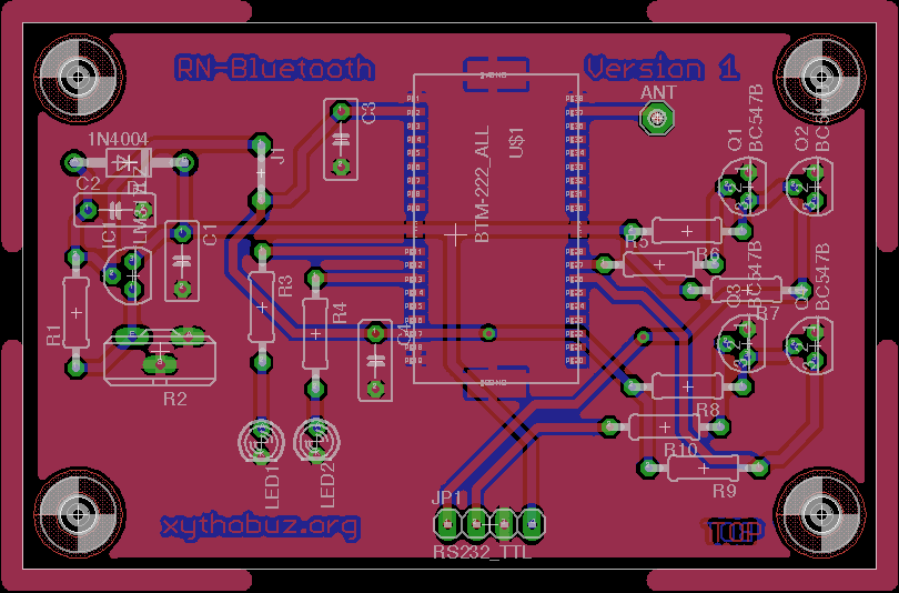
Sd Card Layout Guidelines
Flexible content insights (such as more items, zoom, or different levels of detail) V ol maximum is 0.125 ×v sd and v il maximum is 0.25 ×v sd in ref.
Sd Card Layout Guidelines Understanding Mobile Phones
Keep all spi layout traces as short as possible.

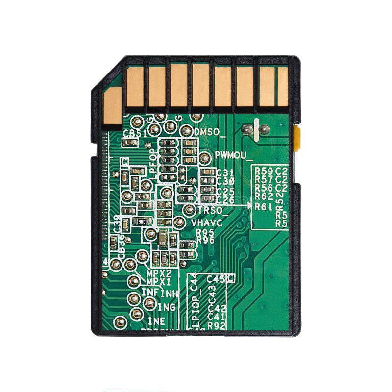
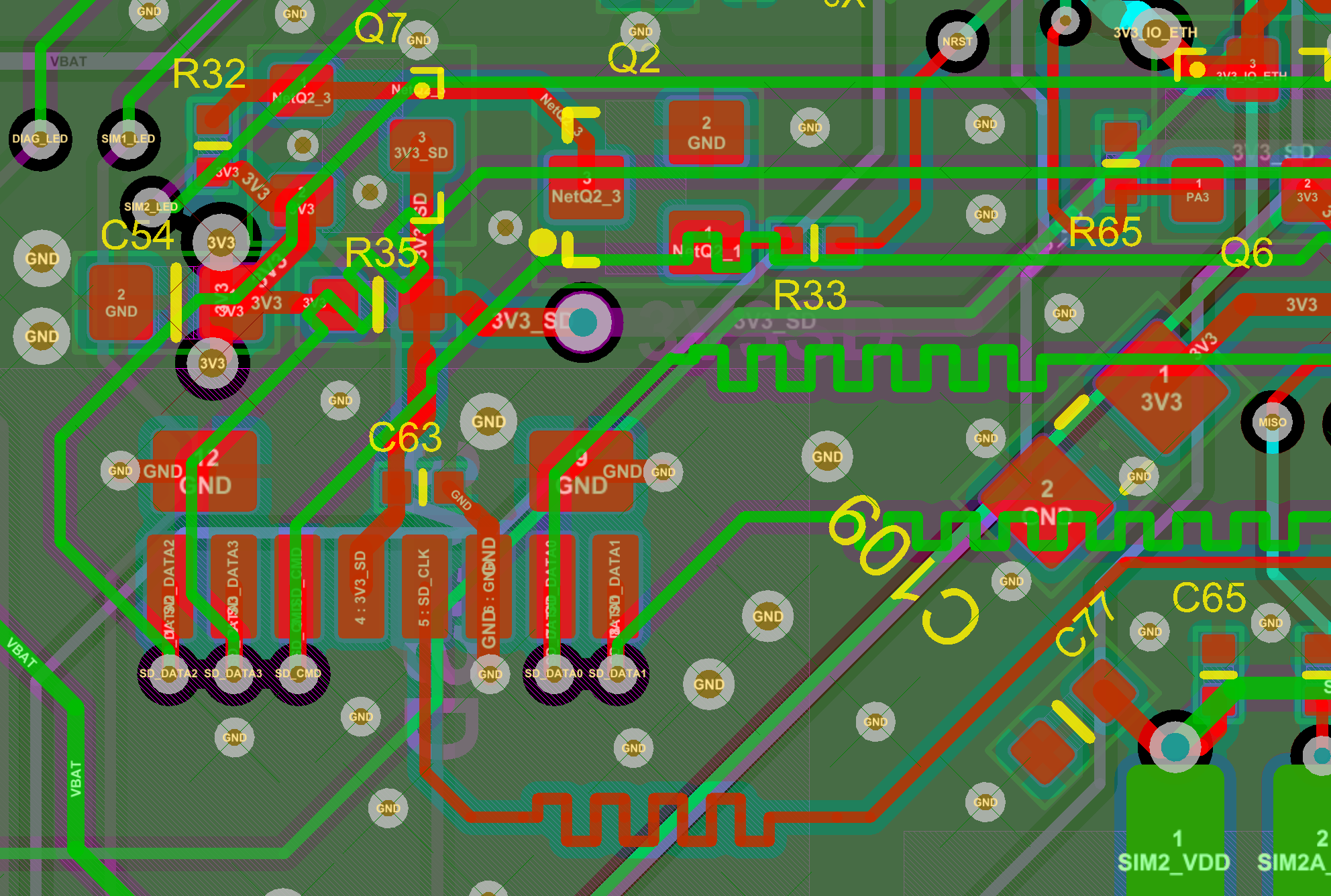
Sd card layout guidelines. Sd card pin assignments [2]. For example, a micro sd card's connector has areas marked with 'no conductive traces' on its datasheet. Not much in terms of detail regarding required layout, the tech sheet just states keep the signals as short as possible.
Sd cards support three protocols, two classes of which are distinct from each other. This document is intended for audiences familiar with pcb manufacturing, layout, and design. In a pcb layout, a few important guidelines must be adhered to for tvs diodes to function efficiently.
Layout guidelines for ddr3 sdram wide interface (>72 bits). 10 ns, data signals at the controller are switched; Please make it far away from other signals to avoid the noise crosstalk.
Secondary reference option where a solid continuous ground reference is also present. The need for multiple lines between the microcontroller and peripheral makes component mounting more of an issue and they should be placed as close together as possible to minimize trace lengths. • provide decoupling capacitance on vdd as per an0002 hardware design considerations.
In the physical layout, the lpddr4 chip is placed on the top side, the data traces are not necessarily connected to the lpddr4 chips in sequential order, but for ease of routing, are connected as best determined by the layout and other critical traces. 1 ns, rising clock edge arrives to the card; As the connector has a moving mechanism, the areas may potentially be scratched and any underlying traces will be damaged in the process.
Twl1200 pcb design guidelines jason battle. Avoid connecting both the tvs diode and the transceiver to a similar ground. 2.5.3 add a 4.7 f capacitor at sd card power (pmos) trace and close to sd card connector.
Recommended pcb routing guidelines for s34mlxx slc nand flash memory figure 3 tsop land pattern (x8, x16) 4 terminationresistors topology the following general guidelines must be considered spacing. Fixed card width and predefined height: Sd_clk termination resistor must be placed close, within 400 mils to socket for four layers pcb.
21 ns, rising clock edge arrives to the card, data is sampled. Usb hardware design guidelines usb connection silabs.com | building a more connected world. Nexperia v oh minimum is 0.7 ×v sd.
This may cause the surge to be channeled to the digital ground, thus causing a ground bounce. Esp32 hardware design guidelines v3.2. Keep all spi layout traces the same length
I.mx28 layout and design guidelines, rev. Users can influence the card size individually: Instead, the transient voltage suppressor should be connected to chassis.
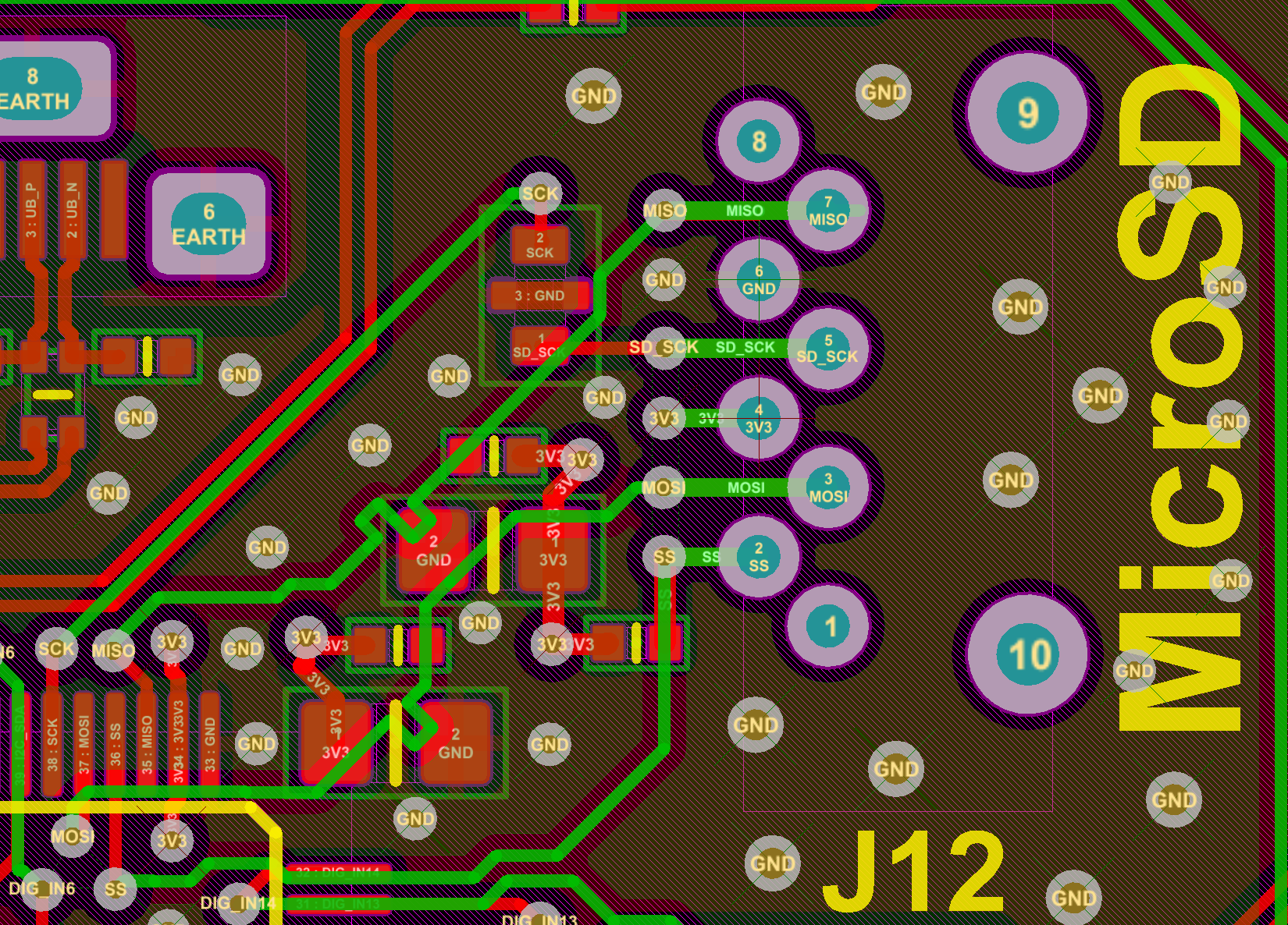
Sd card slot (j12) there is one sd card connector (j12) on the i.mx 8quadxplus mek board. The store sells sd memory cards. I can place it about 1 from the driver, can i simply route it.
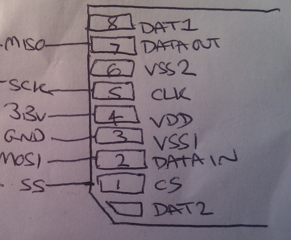
Voh minimum is 0.75 ×vsd and vih minimum is 0.625 ×vsd in ref. The descriptions listed describe the pin functions for each of these two major modes, sd mode and spi mode. • use an esd protection device.
No responsibility is assumed by the sd card association for any damages, any infringements of patents or other right of the sd card association or any third parties, which may result from its use. 2.5 card interface signal 2.5.1 the space of two adjacent trace should be greater than double of trace width (2w rule) 2.5.2 gl823's pin "sd_clk" is clock signals. Design guide v1.1 2 revision history rev date notes 0.1 jan 29, 2016 initial release 1.0 march 2nd, 2016 first release 1.1 sep 9, 2016 change uart, i2s and sdio to 3.3v
The recommended setting for the rc delay circuit is usually r = 10 kω and c = 1 f. 24 ns, hold time ends (3ns after rising clock at the card) • place the ground connections of the dcdc_batt inpu t capacitors as close as possible to both the
18 ns, input setup time starts (3ns before rising clock at the card) 20 ns, rising clock edge at the controller; 5 5 4 4 3 3 2 2 1 1 d d c c b b a a

Sd Card Layout Guidelines PCB

Sd Card Pcb Layout Guidelines PCB Circuits

Micro Usb Pcb Layout PCB Circuits
Sd Card Layout Guidelines Understanding Mobile Phones
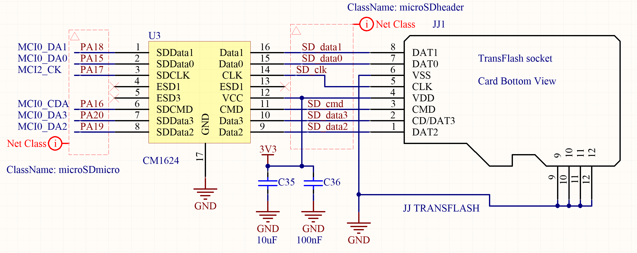
How to design the microSD circuitry


Sd Card Pcb Layout PCB Circuits

Sd Card Layout Guidelines PCB

FPGA SoC Family Intel Mouser 대한민국

Sd Card Pcb Layout Guidelines PCB Circuits
Emi Filter Pcb Layout Guidelines PCB Circuits
Sd Card Pcb Layout Guidelines PCB Circuits
Uart Pcb Layout Guidelines PCB Circuits
Sd Card Pcb Layout PCB Circuits

Sd Card Layout Guidelines PCB

Sd Card Pcb Layout Guidelines PCB Circuits

Sd Card Layout Guidelines PCB
Sd Card Pcb Layout Guidelines PCB Circuits

Micro Sd Card Pcb Layout Circuit Boards

Sd Card Pcb Layout Guidelines PCB Circuits
